

随着物联网的快速发展,无线传感器网络在数据采集、工业控制等方面广泛应用。而在无线传感器网络中,太阳能电源管理电路的设计尤为重要,它决定了无线传感器节点的长期稳定工作和能源利用效率。
With the rapid development of the Internet of Things, wireless sensor networks are widely used in data acquisition, industrial control, and other fields. In wireless sensor networks, the design of solar power management circuits is particularly important because it determines the long-term stable operation and energy utilization efficiency of wireless sensor nodes.
太阳能电源管理电路通常由单晶硅太阳能电池板、超级电容、铅蓄电池、微控制器电路、DCDC电路等部分组成。其中,DCDC电路需要具备可升压降压特性和高转化率,因此我们选择了Sepic电路拓扑结构。该电路具有升降压特性、输入输出同极性和低端驱动开关元件等特点,可实现输入电压Vin在1V-7V范围内,输出电压Vout在0.5V-5V范围内,输出电流Iout在10mA-600mA范围内。同时,为了保证电路的稳定性,我们选用了可供选择的微碧(VBsemi)MOS管型号,如VBZE9N03、VBZE80N03、VBZE40N03、VBZE30N02、VBE1206等,以保证MOS管能承受所经的峰值电压和峰值电流,并尽量减少耗散功率。
Solar power management circuits typically consist of a monocrystalline silicon solar panel, supercapacitors, lead-acid batteries, microcontroller circuits, DCDC circuits, and other components. Among them, the DCDC circuit needs to have boost and buck characteristics and high conversion efficiency. Therefore, we chose the Sepic circuit topology. This circuit has boost and buck characteristics, same polarity input and output, and low-side drive switch elements. It can achieve an input voltage range of Vin from 1V to 7V, an output voltage range of Vout from 0.5V to 5V, and an output current range of Iout from 10mA to 600mA. At the same time, to ensure the stability of the circuit, we selected 微碧(VBsemi) MOSFETs, such as VBZE9N03, VBZE80N03, VBZE40N03, VBZE30N02, VBE1206, etc., to ensure that the MOSFET can withstand the peak voltage and current and minimize power dissipation.
太阳能电源管理电路还需要实现充电和放电保护,以及最大功率点跟踪(MPPT)。为此,我们采用了两级能量机构,即主级能量储存单位铅蓄电池和次级能量储存单位超级电容,构成双能量储存结构,以提高太阳能面板的输出能量利用率。同时,通过对DCDC电路输出电流的采样和单片机调节PWM,实现太阳能电池板的MPPT。在电源路径管理电路中,MOS管开关S1、S2、S3的导通和闭合实现了系统能量流动的控制,可通过微控制器编程实现。
Solar power management circuits also need to implement charging and discharging protection and maximum power point tracking (MPPT). Therefore, we adopted a two-stage energy structure, namely the main energy storage unit lead-acid battery and the secondary energy storage unit supercapacitor, to form a dual-energy storage structure to improve the output energy utilization efficiency of the solar panel. At the same time, by sampling the DCDC circuit output current and adjusting the PWM of the microcontroller, MPPT of the solar panel can be achieved. In the power path management circuit, the conduction and closure of MOSFET switches S1, S2, and S3 control the energy flow of the system and can be programmed through the microcontroller.
下面是太阳能电源管理电路的整体结构图、Sepic电路拓扑结构图、电源路径管理电路图和可供选择的微碧(VBsemi)MOS管型号图。
Below are the overall structure diagram of the solar power management circuit, Sepic circuit topology diagram, power path management circuit diagram, and 微碧(VBsemi) MOSFET model diagram.
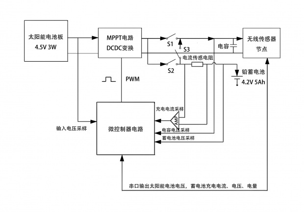
【太阳能电源管理电路整体结构图】
[Overall structure diagram of the solar power management circuit]
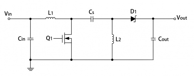
【Sepic电路拓扑结构图】
[Sepic circuit topology diagram]
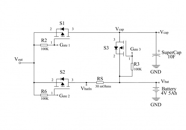
【电源路径管理电路图】
[Power path management circuit diagram]
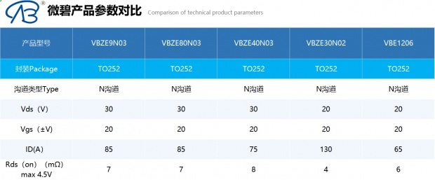
【可供选择的微碧(VBsemi)MOS管型号图】
[微碧(VBsemi) MOSFET model diagram]
在实际应用中,该电源管理电路的转换率高达80%以上,静态工作电流小于1mA,能源利用率高、寿命长、合理分配输出能量等特点,成本低廉、稳定性和可靠度高。因此,该电源管理电路在无线传感器网络中的应用前景广阔,有望成为未来无线传感器网络能源管理的重要发展方向。
In practical applications, the conversion rate of the power management circuit is as high as 80% or more, the static working current is less than 1mA, and it has the advantages of high energy utilization efficiency, long service life, reasonable distribution of output energy, low cost, high stability, and reliability. Therefore, the power management circuit has broad prospects for application in wireless sensor networks and is expected to become an important development direction for future energy management of wireless sensor networks.
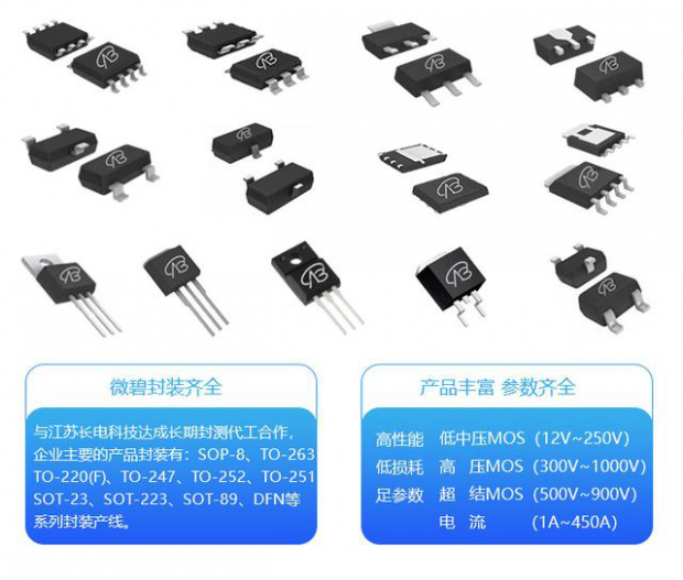
【微碧部分MOS管产品封装图】
[Microgreen MOSFET product packaging diagram]